
![[Italian]](images/uk.gif)


PCMCIA Switch Controller
The goal of the work is the implementation of the control logic and interface between PC, Switches (Mindspeed boards) and the u-Blox GPS expansion board. This interface is realized through a PCMCIA board that is based on a Xilinx XC3S400 FPGA. This FPGA board should replace the one that is previously used in the IP-Flow testbed.
The aim of the IP-Flow project is to allow long distance transmission of data on high rate switching data-links: the hardware must be able to perform switching operation on two separate switches at the same time (the tolerance is of some nanoseconds).
In order to guarantee the required precision a GPS reference PPS (Pulse per Second) will be used in order to generate and deliver precise and stable frequency and time reference signals. This is fundamental to synchronize two different devices in all over the world.
The reference FPGA board can transfer data on the PCMCIA interface in order to communicate with the PC (really it is using the faster CardBus protocol, which is an evolution of the PCMCIA one). Furthermore there is an expansion slot (on the other side of the board) used to connect the uBlox GPS receiver and the mindspeeds interfaces.
1 - Hardware description
Here follows a short description of the material implied in the project and described in this document:
- ComBlock COM1300-C FPGA board (link)
- 3TEC expansion board
1.1 - ComBlock COM1300-C board
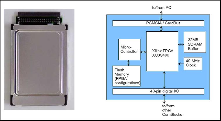
The board is a small FPGA board, which main feature is to be interfaceable with a PC like a PCMCIA. Really the board is not using the PCMCIA protocol, but the newest and more advanced CardBus protocol.
The COM1300-C is 32-bit CardBus Type II (5mm height) card for custom application development. The main parts of the board are a Spartan-3 FPGA and SDRAM memory chip. This parts are also supplied by a 40[MHz] clock, a Micro-Controller, a Flash Memory that stores the FPGA configurations, a 40-pin extension connector and obviously the CardBus interface.
The main development context of the COM1300-C board is on the ComBlock project to supply small commercial off-the-shelf modules with essential communication processing functions, including modulation, demodulation, error correction encoding and decoding, digital to analog/RF, RF/analog to digital, formatting, data storage and base-band interfaces. In any case the board can be used standalone and the extension connector can be used to interface other parts instead of the ComBlock blocks. In our case this extension connector will be used to connect the "3TEC expansion board", which permits to reach the GPS module and the Mindspeed switch connectors.
|
The detailed description of the blocks of the PCMCIA card follow:
- CardBus
CardBus are PCMCIA 2.1 or later 32-bit PCMCIA cards, introduced in 1995. CardBus is a 32-bit, 33 MHz PCI bus in the PC card form factor. CardBus interface is typically used on laptop PCs. CardBus peripheral instance are mobile modems and Wi-Fi interfaces. Typical sustained data throughputs are 100/40 Mbits/s.
- SDRAM
The board is provided with a 32MB SDRAM to be used as elastic buffer. A future employment of this SDRAM in the IP-Flow project will be to store huge switching tables.
- Clock
The card is populated with a 40 MHz oscillator that supplies the main clock signal directly to the FPGA.
- Micro-Controller
On the board there is an ATmega8515L-8AC micro-controller that is used to manage the CardBus interface and to redirect the data addressed to the Flash Memory.
- Flash Memory
The FPGA configuration is stored in a non-volatile Flash Mmory. ComBlock supplies the ComBlock Control Center that is a software utility to write a “.mcs” PROM file into the flash memory over the selected communication link between host computer and COM-1300. This “.mcs” PROM file can be created through compiling the architecture in the Xilinx ISE toolset and will be the way to program the Spartan-3 FPGA.
At power up, the FPGA is automatically programmed with the configuration file stored within the flash memory. Configuring the FPGA takes approximately 0.4 seconds.
The COM-1300 is protected against corruption by an invalid FPGA configuration file. To recover from such occurrence is enough to connect the BOOT SECTOR pin (that is the A20 of the expansion connector) to ground (pin B20) and plug in the card. The card will be automatically configured with a default FPGA configuration that restores CardBus communication. This boot file is not erasable. Once this is done, the user can safely re-load a valid FPGA configuration file into flash memory using the ComBlock Control Center.
Up to 14 distinct custom FPGA configurations can be retained in the Flash memory. The user can select which configuration is to be loaded at power up through the ComBlock Control Center. A change in the FPGA configuration, whether from the graphical user interface or by software command, necessitates the removal and re-insertion of the PCMCIA/CardBus card into the slot.- Expansion Connector
On the other side of the CardBus connector the card is populated with a 40-pin expansion slot. Each of the pins is named from A1 to B20. Most of the pins are general purpose and its functionalities can be depicted by the FPGA.
The A1 pin can be used to give an external clock to the FPGA, an alternative to the internal 40 MHz clock. The A18 and B18 pins are depicted to asynchronous serial communication with other external blocks. The A20 pin is for the BOOT SECTOR signal. Connecting it to ground (e.g. B20) and plug in the card to re-activate the default FPGA configuration. B5, B10, B15 and B20 pins are connected to the ground.- Spartan-3 FPGA
The FPGA located on the card is a Spartan-3 XC3S400 in the FT256 package with 400K system gates.
1.2 - 3TEC expansion board
The “3TEC expansion board” is primary used for two scope:
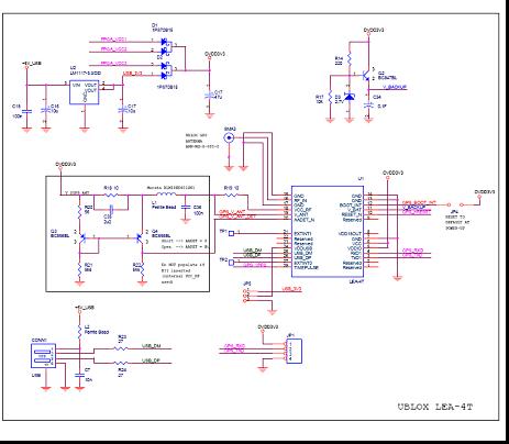
- The first one is to place and to interconnect the uBlox GPS module that gives the reference PPS signal. In order to achieve this target, the expansion board is provided with the necessary surrounding hardware, starting from the power supply circuitry until the antenna connector
- The second aim of the expansion board is to house the mindspeed connectors, which permits the FPGA to communicate with them. The mindspeed connectors and interface features are the same as in the previous testbed stuff (see the document named “GigaEthernetSwitching FPGA-based control”)
Obviously the “3TEC expansion board” has also the 40-pin connector that will be coupled with the PCMCIA board one.
|
2 - Hardware Interconnections
To recreate the behavior described in this document it’s simply required to connect the expansion board with the ComBlock COM1300-C and plug in the PCMCIA slot of a PC. Two Mindspeed switches can be connected to the two connectors available on the expansion board.|
Pages hosted by "IP-FLOW Group" - DIT - Università di Trento - Italy. © IP-FLOW Project 2004, All Rights Reserved. Last updated: 2008-09-10 05:37:04 |